- 您现在的位置:买卖IC网 > Sheet目录1998 > ICS844002AG-01LF (IDT, Integrated Device Technology Inc)IC SYNTHESIZER 2LVDS 20-TSSOP
ICS844002-01
FEMTOCLOCKS CRYSTAL-TO-LVDS FREQUENCY SYNTHESIZER
IDT / ICS LVDS FREQUENCY SYNTHESIZER
8
ICS844002AG-01 REV. A SEPTEMBER 28, 2007
Parameter Measurement Information, continued
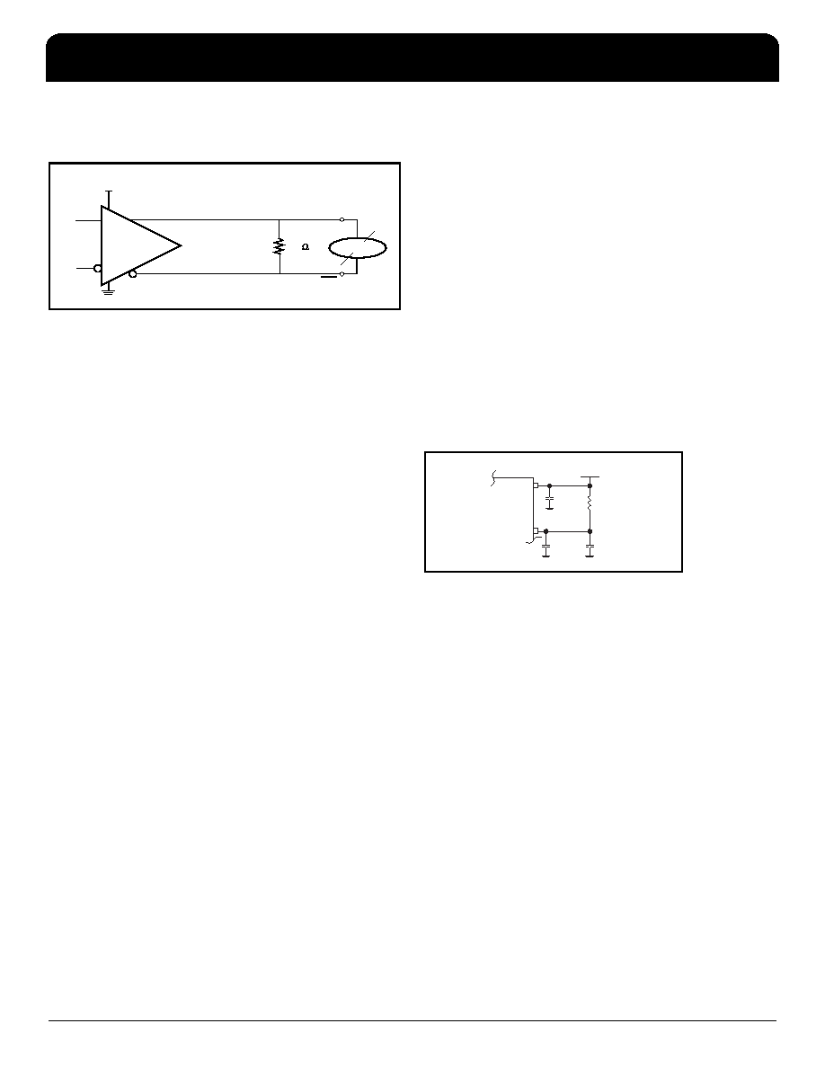
Differential Offset Voltage Setup
Application Information
Power Supply Filtering Technique
As in any high speed analog circuitry, the power supply pins are
vulnerable to random noise. The ICS844002-01 provides separate
power supplies to isolate any high switching noise from the outputs
to the internal PLL. VDD, VDDA and VDDO should be individually
connected to the power supply plane through vias, and bypass
capacitors should be used for each pin. To achieve optimum jitter
performance, power supply isolation is required. Figure 1
illustrates how a 10
resistor along with a 10F and a 0.01F
bypass capacitor should be connected to each VDDA pin.
Figure 1. Power Supply Filtering
Recommendations for Unused Input and Output Pins
Inputs:
LVCMOS Control Pins
All control pins have internal pull-ups or pull-downs; additional
resistance is not required but can be added for additional
protection. A 1k
resistor can be used.
REF_CLK INPUT
For applications not requiring the use of the reference clock,
it can be left floating. Though not required, but for additional
protection, a 1k
resistor can be tied from the REF_CLK to
ground.
Crystal Inputs
For applications not requiring the use of the crystal oscillator input,
both XTAL_IN and XTAL_OUT can be left floating. Though not
required, but for additional protection, a 1k
resistor can be tied
from XTAL_IN to ground.
Outputs:
LVDS Outputs
All unused LVDS output pairs can be either left floating or
terminated with 100
across. If they are left floating, we
recommend that there is no trace attached.
100
out
LVDS
DC Input
VOD/ VOD
V
DD
VDD
VDDA
3.3V or 2.5V
10
10F
.01F
发布紧急采购,3分钟左右您将得到回复。
相关PDF资料
ICS844002AGI-01LFT
IC SYNTHESIZER 2LVDS 20-TSSOP
ICS844002AGLF
IC SYNTHESIZER 2LVDS 20-TSSOP
ICS844004AK-104LF
IC SYNTHESIZER LVDS 32-VFQFPN
ICS844004AKI-104LFT
IC SYNTHESIZER LVDS 32-VFQFPN
ICS844021BG-01LFT
IC CLOCK GEN ETHERNET 8-TSSOP
ICS844021BGI-01LFT
IC CLOCK GEN ETHERNET 8-TSSOP
ICS844071AGLFT
IC CLOCK GEN GIG ETH 8-TSSOP
ICS844201BG-45LF
IC CLK GENERATOR 25MHZ 8TSSOP
相关代理商/技术参数
ICS844002AG-01LFT
功能描述:IC SYNTHESIZER 2LVDS 20-TSSOP RoHS:是 类别:集成电路 (IC) >> 时钟/计时 - 时钟发生器,PLL,频率合成器 系列:HiPerClockS™, FemtoClock™ 标准包装:1,000 系列:- 类型:时钟/频率合成器,扇出分配 PLL:- 输入:- 输出:- 电路数:- 比率 - 输入:输出:- 差分 - 输入:输出:- 频率 - 最大:- 除法器/乘法器:- 电源电压:- 工作温度:- 安装类型:表面贴装 封装/外壳:56-VFQFN 裸露焊盘 供应商设备封装:56-VFQFP-EP(8x8) 包装:带卷 (TR) 其它名称:844S012AKI-01LFT
ICS844002AGI-01LF
功能描述:IC SYNTHESIZER 2LVDS 20-TSSOP RoHS:是 类别:集成电路 (IC) >> 时钟/计时 - 时钟发生器,PLL,频率合成器 系列:HiPerClockS™, FemtoClock™ 标准包装:1,000 系列:Precision Edge® 类型:时钟/频率合成器 PLL:无 输入:CML,PECL 输出:CML 电路数:1 比率 - 输入:输出:2:1 差分 - 输入:输出:是/是 频率 - 最大:10.7GHz 除法器/乘法器:无/无 电源电压:2.375 V ~ 3.6 V 工作温度:-40°C ~ 85°C 安装类型:表面贴装 封装/外壳:16-VFQFN 裸露焊盘,16-MLF? 供应商设备封装:16-MLF?(3x3) 包装:带卷 (TR) 其它名称:SY58052UMGTRSY58052UMGTR-ND
ICS844002AGI-01LFT
功能描述:IC SYNTHESIZER 2LVDS 20-TSSOP RoHS:是 类别:集成电路 (IC) >> 时钟/计时 - 时钟发生器,PLL,频率合成器 系列:HiPerClockS™, FemtoClock™ 标准包装:1,000 系列:- 类型:时钟/频率合成器,扇出分配 PLL:- 输入:- 输出:- 电路数:- 比率 - 输入:输出:- 差分 - 输入:输出:- 频率 - 最大:- 除法器/乘法器:- 电源电压:- 工作温度:- 安装类型:表面贴装 封装/外壳:56-VFQFN 裸露焊盘 供应商设备封装:56-VFQFP-EP(8x8) 包装:带卷 (TR) 其它名称:844S012AKI-01LFT
ICS844002AGILF
功能描述:IC SYNTHESIZER 2LVDS 20-TSSOP RoHS:是 类别:集成电路 (IC) >> 时钟/计时 - 时钟发生器,PLL,频率合成器 系列:HiPerClockS™, FemtoClock™ 标准包装:27 系列:Precision Edge® 类型:频率合成器 PLL:是 输入:PECL,晶体 输出:PECL 电路数:1 比率 - 输入:输出:1:1 差分 - 输入:输出:无/是 频率 - 最大:800MHz 除法器/乘法器:是/无 电源电压:3.135 V ~ 5.25 V 工作温度:0°C ~ 85°C 安装类型:表面贴装 封装/外壳:28-SOIC(0.295",7.50mm 宽) 供应商设备封装:28-SOIC 包装:管件
ICS844002AGILFT
功能描述:IC SYNTHESIZER 2LVDS 20-TSSOP RoHS:是 类别:集成电路 (IC) >> 时钟/计时 - 时钟发生器,PLL,频率合成器 系列:HiPerClockS™, FemtoClock™ 标准包装:1,000 系列:- 类型:时钟/频率合成器,扇出分配 PLL:- 输入:- 输出:- 电路数:- 比率 - 输入:输出:- 差分 - 输入:输出:- 频率 - 最大:- 除法器/乘法器:- 电源电压:- 工作温度:- 安装类型:表面贴装 封装/外壳:56-VFQFN 裸露焊盘 供应商设备封装:56-VFQFP-EP(8x8) 包装:带卷 (TR) 其它名称:844S012AKI-01LFT
ICS844002AGLF
功能描述:IC SYNTHESIZER 2LVDS 20-TSSOP RoHS:是 类别:集成电路 (IC) >> 时钟/计时 - 时钟发生器,PLL,频率合成器 系列:HiPerClockS™, FemtoClock™ 标准包装:1,000 系列:- 类型:时钟/频率合成器,扇出分配 PLL:- 输入:- 输出:- 电路数:- 比率 - 输入:输出:- 差分 - 输入:输出:- 频率 - 最大:- 除法器/乘法器:- 电源电压:- 工作温度:- 安装类型:表面贴装 封装/外壳:56-VFQFN 裸露焊盘 供应商设备封装:56-VFQFP-EP(8x8) 包装:带卷 (TR) 其它名称:844S012AKI-01LFT
ICS844002AGLFT
功能描述:IC SYNTHESIZER 2LVDS 20-TSSOP RoHS:是 类别:集成电路 (IC) >> 时钟/计时 - 时钟发生器,PLL,频率合成器 系列:HiPerClockS™, FemtoClock™ 标准包装:1,000 系列:- 类型:时钟/频率合成器,扇出分配 PLL:- 输入:- 输出:- 电路数:- 比率 - 输入:输出:- 差分 - 输入:输出:- 频率 - 最大:- 除法器/乘法器:- 电源电压:- 工作温度:- 安装类型:表面贴装 封装/外壳:56-VFQFN 裸露焊盘 供应商设备封装:56-VFQFP-EP(8x8) 包装:带卷 (TR) 其它名称:844S012AKI-01LFT
ICS844002AKLF
功能描述:IC SYNTHESIZER 2LVDS 32-VFQFPN RoHS:是 类别:集成电路 (IC) >> 时钟/计时 - 时钟发生器,PLL,频率合成器 系列:HiPerClockS™, FemtoClock™ 标准包装:1,000 系列:- 类型:时钟/频率合成器,扇出分配 PLL:- 输入:- 输出:- 电路数:- 比率 - 输入:输出:- 差分 - 输入:输出:- 频率 - 最大:- 除法器/乘法器:- 电源电压:- 工作温度:- 安装类型:表面贴装 封装/外壳:56-VFQFN 裸露焊盘 供应商设备封装:56-VFQFP-EP(8x8) 包装:带卷 (TR) 其它名称:844S012AKI-01LFT